
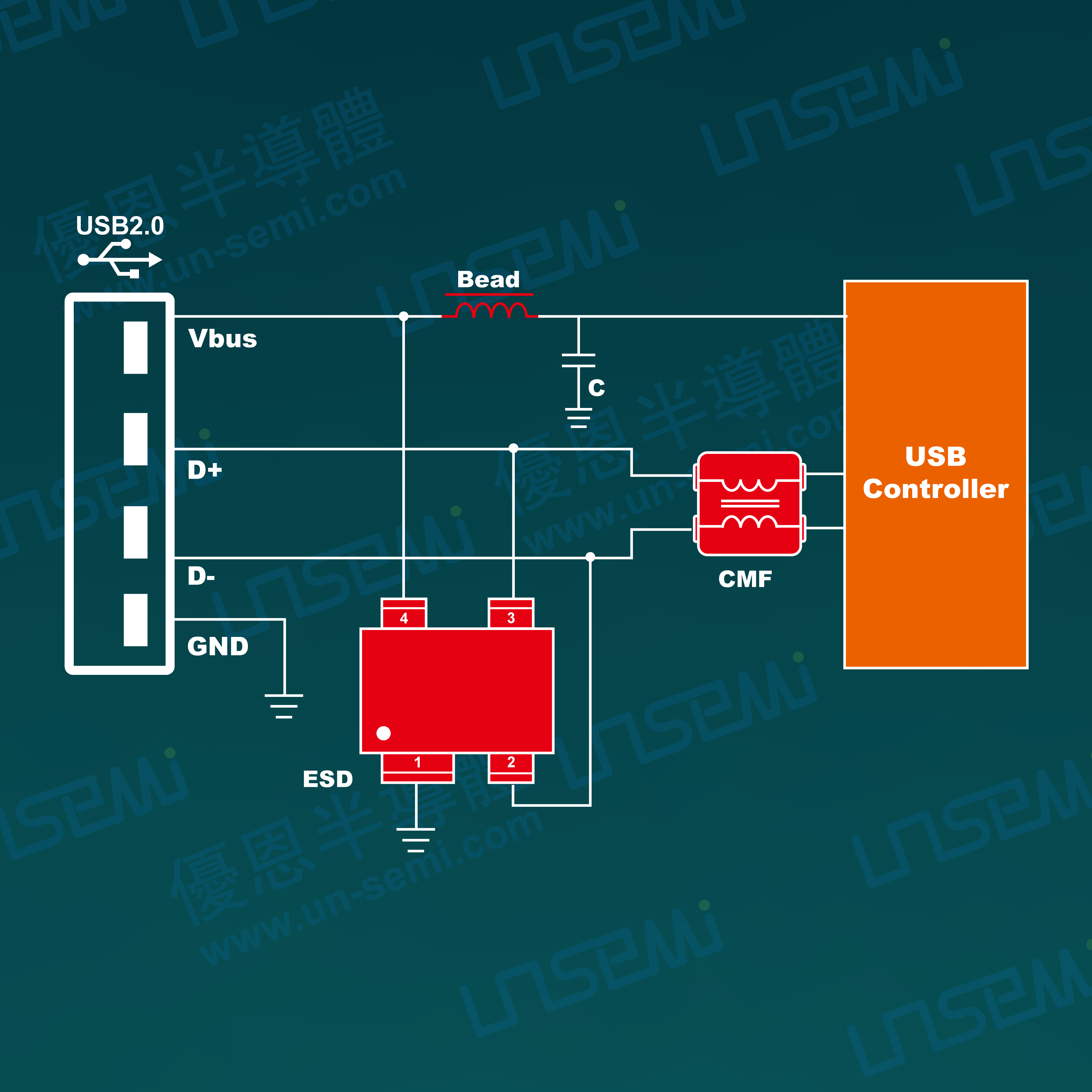
USB 2.0 is a widely used high-speed serial interface standard. With its high-speed transmission, wide compatibility, and ease of use, it has become a core technology for connecting electronic devices. It is widely used in storage devices such as USB flash drives and external hard drives; peripheral devices such as mice, keyboards, printers, and scanners; multimedia devices such as smartphones, tablets, digital cameras, and camcorders; and industrial equipment control. It can achieve data transmission speeds up to 480Mbps and provide power. Due to the frequent hot-plugging of USB 2.0 interfaces, they are susceptible to electrostatic discharge (ESD), overcurrent (such as from peripheral short circuits), and surges (due to transients during plug-in and unplugging, as well as coupling from power grid interference). Furthermore, the high-speed differential signal is susceptible to electromagnetic interference (EMI), which can cause transmission errors, leading to device recognition errors, communication interruptions, chip damage, and even host device failure. To protect the USB 2.0 interface and associated systems, multiple layers of protection must be implemented in the interface design. For example, ultra-low-capacitance TVS diodes should be deployed on each signal line at the interface, ferrite beads should be connected in series on the power lines, and noise filters should be connected in series on the differential pairs,and combined with good grounding and shielding design, reasonable protection design can significantly improve device reliability, extend device service life, and ensure long-term stable system operation.
IEC 61000-4-2、EN 61000-4-2、GB/T 17626.2
1. The back-end IC is protected by connecting silicon ESD protection device with high voltage accuracy, fast response speed, low clamping voltage and low junction capacitance in parallel in the circuit;
2. Connect ferrite beads in series on the power line and noise filters in series on the differential signal line can effectively suppress EMI electromagnetic noise interference;
3. Meet the requirements of EMC design without affecting data transmission, so that the system circuit can be effectively and comprehensively protected.
▲The scheme for reference only. Please feel free to contact us if you need a detaile solution or customization according to your protection level requirements, We will provide professional technical support and solutions based on your specific needs.
| Part Number | Package | Impedance (Ω) |
Z Test Freq. (MHz) |
DCR Max.(Ω) |
Rated Current Max.(mA) |
Datasheet |
|---|
| Part Number | Package | Imp.Com. (Ω)±25% @100MHz |
DCR Max.(Ω) |
Rated Current Max.(mA) |
Rated Voltage (V) |
Withstand Voltage (V) |
Insulation Resistance Min.(MΩ) |
Datasheet |
|---|
| Part Number | Package | Impedance (Ω) |
Z Test Freq. (MHz) |
DCR Max.(Ω) |
Rated Current Max.(mA) |
Datasheet |
|---|
| Part Number | Package | Impedance (Ω) |
Z Test Freq. (MHz) |
DCR Max.(Ω) |
Rated Current Max.(mA) |
Datasheet |
|---|
| Part Number | Package | Imp.Com. (Ω)±25% @100MHz |
DCR Max.(Ω) |
Rated Current Max.(mA) |
Rated Voltage (V) |
Withstand Voltage (V) |
Insulation Resistance Min.(MΩ) |
Datasheet |
|---|
| Part Number | Package | VRWM Max. (V) |
VBR Min. (V) |
Vc @1A (V) |
IPP Max. (A) |
CJ@ 1MHZ (PF) |
IR@VRWM Max. (uA) |
Protectable Lines |
AEC-Q101 | Datasheet |
|---|


